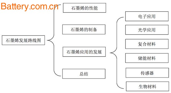
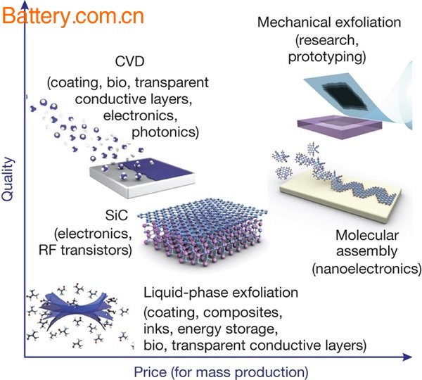
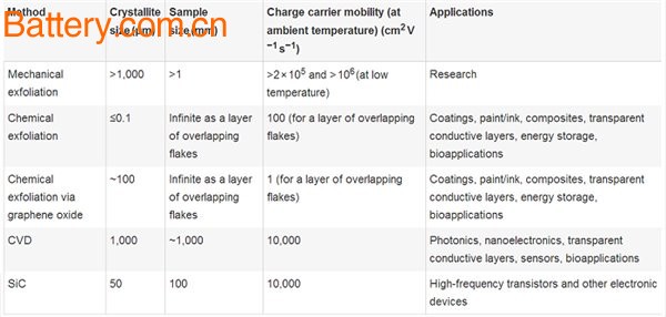
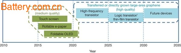
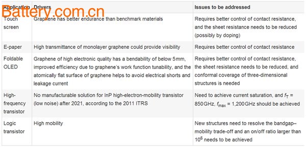
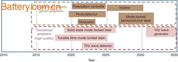
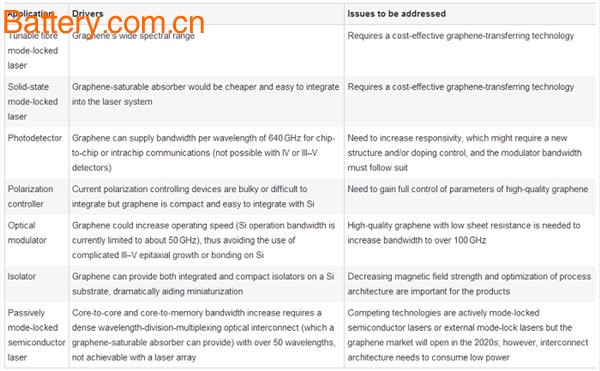
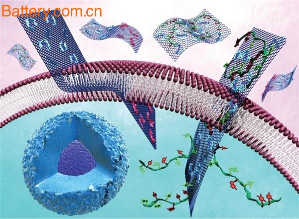
In recent years, many breakthroughs have been made in the study of graphene (the first two-dimensional atomic crystal), and significant progress has been made in the preparation of graphene. This one-atom carbon material combines many excellent properties such as high mechanical strength, electrical conductivity, thermal conductivity and impermeability, which makes it attractive in many fields. KSNovoselov, who won the 2010 Nobel Prize in Physics for his outstanding research in graphene materials, was invited to write a review on the latest developments in graphene. The review was published in October 2012 with the title "A roadmap for graphene". Published in the Nature Journal on the 11th. This review reviews recent advances in graphene research, reviews the development of preparation methods, and critically analyzes the feasibility of various applications of graphene. Let's take a look at it now! â–²KSNovoselov, one of the winners of the 2010 Nobel Prize in Physics 1 Introduction Can graphene be the next generation of disruptive technology, replacing some of the materials currently in use, and opening up new markets? Is it versatile enough to make a breakthrough in every aspect of our lives? From the nature of graphene, it does have this potential. Graphene is the first two-dimensional atomic crystal prepared by scientists. Many of its parameters – such as stiffness, strength, elasticity, electrical conductivity, thermal conductivity, etc. – are unparalleled. These properties indicate that graphene can replace many other materials. However, the fact that so many excellent features are concentrated on this material means that graphene will likely lead to revolutionary technology. The transparency, conductivity and elasticity of graphene make it suitable for flexible electronic devices, and its transparency, impermeability and electrical conductivity make it suitable for transparent protective films and separators; the combined application of this property is becoming more and more many. However, the application of new technologies is usually a long and costly process. Is the nature of graphene special enough to be universal enough to change the status quo and turn to more convenient new technologies? â–²Overview navigation map 2, graphene properties One of the reasons why graphene has developed so rapidly is that researchers can obtain high quality graphene in the laboratory through relatively simple and low cost methods. Many of the properties of graphene have exceeded the performance of other materials, and some properties have even reached the theoretical prediction limit. For example, the room temperature electron mobility is 2.5x105cm2V-1s-1 (theoretical value is 2x105cm2V-1s-1); the Young's modulus is 1TPa, the intrinsic intensity is 130GPa (very close to the theoretical value); high thermal conductivity ( Above 3000WMK-1); optical absorption rate is πα≈2.3% (α is constant); airtight, can maintain very high current ( many times higher than copper). It is another characteristic of graphene that can carry functionalized functional groups. Graphene has earned the title of "Miracle Material" for its many excellent properties. However, these excellent properties are based on high quality samples (mechanically exfoliated graphene), and graphene needs to be stored on a special substrate such as hexagonal boron nitride. So far, the same performance has not been obtained by using graphene of other preparation methods, so this method is rapidly developing. If the performance of industrial graphene can be as excellent as that of graphene prepared in the laboratory, there will be great prospects for industrial applications. There are many two-dimensional crystals in nature, such as boron nitride and molybdenum disulfide, which have the same structure as graphene, but they have their own unique properties. These two-dimensional crystals offer the possibility of materials and equipment for better performance, or can be used in combination with graphene (eg two-dimensional heterostructure materials). Although this review does not cover all two-dimensional crystal materials, graphene still has great commercial value as part of two-dimensional crystal materials and heterostructures. 3, preparation problems The production of graphene with special applications is the key to the graphene application market, and this situation will last for ten years or until the performance of graphene can meet the potential applications of graphene. Many methods for preparing multi-dimensional, various shapes and high quality graphenes have been developed. Only the preparation methods that can be used for mass production are focused here. Graphene is classified into the following categories according to the properties of graphene: (1) graphene or reduced graphene oxide sheets for composite materials, conductive coatings, etc.; (2) planar graphene for low activity and stable equipment; (3) Planar graphene for high performance electronic devices. The performance of different types of graphene depends heavily on the quality of the material, such as defects, substrates, etc., and is greatly affected by the processing method. (See Figure 1 and Table 1) â–² Figure 1 The cost performance of different methods for preparing graphene by macro 3.1 Liquid phase and thermal stripping The liquid phase exfoliated graphene (or other layered material) is obtained by a method of increasing the crystal area of ​​graphene by the surface tension of the solvent. The solvent may be selected from a conventional nonaqueous solution solvent, and a surfactant may be added to the aqueous solvent. By ultrasonic dispersion, graphene is separated into individual platelets, and the time of ultrasonication can be extended to obtain more single-layer tablets in the suspension, and the content of the single-layer tablets can be further improved by centrifugal separation. The synthetic route of graphene oxide is related to this method, that is, the graphene pellets are first oxidized and then ultrasonically stripped in an aqueous solution. After stripping the graphene oxide, the suspension needs to be further processed by centrifugal dispersion, and then the suspension can be deposited as a film on almost any surface and (partially) reduced to the state of the parent graphene in situ. The preparation method of the complete aqueous solvent graphene oxide used in the industry is carried out by a thermal shock process to complete the stripping and reduction. Although the graphene composition obtained by this method contains many layer structures, it still maintains the excellent properties of single-layer graphene. Similar to the oxidation process, the stacking process of graphite can be disturbed by inserting small molecules. For example, small molecules inserted in graphite are subjected to a treatment process similar to the oxidation process, and then subjected to a heat treatment or a plasma treatment process, so that the graphene is arranged in a single layer. Many graphene nanoribbon suspensions are prepared by pulling apart single-walled carbon nanotubes like a zipper. Although this method is more expensive than the method of chemically stripping graphene or graphene oxide, these methods can result in a suspension of sheetene distribution (narrower) of graphene sheets. At the same time, the nanotube splitting method can better control the quality of chemical functional groups and edges. This method of producing block-level graphene has been used for mass production and is now being evaluated for use in many fields. Therefore, graphene inks and pigments will be used in industries such as electronics, electromagnetic shielding, barrier coating, heat dissipation, and capacitors . Many sheet-based products are expected to enter the market after many years, and the application of conductive inks on the commercial level has been confirmed. 3.2 Chemical vapor deposition The method of preparing a large-area uniform graphene film by chemical vapor deposition (CVD) on a copper foil and a film is being developed, and has shown great promise in many fields. Although the entire preparation process requires the transfer of graphene from a copper substrate to an insulating surface or other substrate, it has been possible to produce square-level graphene. On the latest equipment, graphene films can be transferred to 200mm silicon wafers. On a smaller scale, these films exhibit the same transfer ability as graphene stripped on silica and hexagonal boron nitride substrates. Although this method has defects such as grain boundaries and excessive thickness of the sheet, such a film has been used in a transparent conductive coating (for example, a touch screen). At present, this method is too costly because it requires a large energy consumption to remove the underlying metal layer. Once the transfer process is rationalized, this approach can actually reduce costs. Before the promotion of graphene CVD technology, there are many problems to be solved. It is necessary to control the growth of the graphene on the metal thin film (10 nm) while controlling the crystal size, the doping content, and the number of sheets. Controlling the number and direction of crystallization of the graphene sheets is of the utmost importance because many applications require a two-, three-, or thicker graphene structure. At the same time, this transfer process can be optimized to reduce the destruction of graphene and reducing corrosion of metals. This transfer process can become complicated because of the growth of graphene itself. However, many applications rely on the growth of graphene on a metal surface, without the need for graphene transfer: the high thermal and electrical conductivity of graphene and excellent shielding properties, allowing graphene to enhance copper conductors in closed loops. performance. Because graphene is inert, it can block any gas and form a conformal layer on the surface of any metal surface, which can be used as a corrosion-resistant coating. A breakthrough in the preparation of graphene should be to allow graphene to grow on any surface or at low temperatures (for example, using plasma CVD, etc.) while reducing the number of defects. The former method can avoid complicated and expensive transfer processes and promote the combination of two-dimensional crystals with other materials (such as silicon and gallium arsenide). The latter method can improve the combination with microelectronics technology and can save a lot of energy. 3.3 Synthesis on SiC As a material commonly used for high-power electronic devices, silicon carbide has been confirmed to allow a graphite layer to grow on the surface of carbon or silicon in silicon carbide crystals by sublimation of silicon atoms, thereby obtaining a graphitized surface. First, the carbon terminal of the silicon carbide surface is grown into a randomly oriented multilayer crystal layer, but the amount of graphene layer growth is controlled. This graphene has crystals close to several hundred microns and the quality is better. The two main disadvantages of this method are that the price of silicon carbide crystals is relatively high and the required temperature is higher (above 1000 ° C) due to the poor compatibility of graphite with silicon electronic devices. Further research is needed for this method, and several potential methods for growing graphene on silicon carbide are currently available. Due to the relatively high growth temperature, the substrate is relatively expensive, and the crystal diameter is relatively small, the method for preparing graphene on silicon carbide is limited in application. When the seventh main element material (such as gallium arsenide, gallium carbide, etc.) can reach the limit of 1 THz, graphene based on silicon carbide growth can be well applied to high frequency transistors within ten years. This short transistor is currently widely used in 20 μm crystals (currently obtained by growing graphene in silicon carbide). Another interesting but niche application is that this graphene sample can be used as a measure of resistance. At higher temperatures, this graphene has a higher ratio than the conventional hexagonal structure of gallium arsenide. Resistance accuracy. In addition to the unavoidable problem of high temperatures during the growth process, it is necessary to solve the multi-crystal layer (causing carrier scattering) generated by the edge between the second layer and the third layer during the growth process in the next decade. It is due to the increase in the size of the crystal and the unintentional control of the sinker and buffer layer. 3.4 Other growth methods Although there are many other growth methods, they are unlikely to be used in commercial production in the next decade. However, some of these methods still have certain advantages and require further research. The dehydrocyclization of linear polyphenylene monomer molecular initiators is a chemically driven method for preparing high quality graphene nanoribbons and more complex structures from the bottom up. Molecular beam epitaxy has been used to grow chemically pure graphene, but since the cost is higher than the CVD method, mass production is impossible. Laser ablation is a potential growth technique that allows graphene nanosheets to be deposited on any substrate. However, compared with the method of chemically stripping graphene, the cost is high, so it is not widely used at present. â–¼Table 1 Properties of graphene obtained by different preparation methods 4. Graphene electronic devices Due to the lack of bandgap, it is unlikely that graphene will be made into a planar channel material for high performance integrated circuits within ten years. However, some other graphene applications are being developed using some materials that are not yet ideal in terms of quality. Figures 2 and 2 list some of the devices that have been or will be applied using graphene-based models. â–² Figure 2 Graphene-based display and electronic equipment â–¼Table 2 Electron application of graphene 4.1 Flexible electronic devices Conductive coatings are widely used in electronic products such as touch screens, electronic paper and organic light emitting diodes, and special applications that require low surface resistance and high transmission. Graphene meets the needs of electronic and optical devices, with a single layer transmission rate of 97.7%, but in the past it was considered that the performance of indium tin oxide (ITO) would be better. However, considering the increase in the quality of graphene every year, the price of ITO will be higher, and the cost of ITO prepared by deposition method is also higher, so graphene will definitely get a larger market share. The excellent flexibility and corrosion resistance of graphene is the most important property of flexible electronic materials equipment, but ITO cannot be achieved in this respect. The electrical performance required for motors in different applications is different (such as surface resistance). Due to the different production methods, there are various grades of transparent conductive coatings. Therefore, the electrodes of the touch screen (products requiring CVD) have a relatively high surface conductance based on a light transmittance of 90%. The advantage of the use of graphene electrodes on contact panels is that graphene has greater stability. In addition, graphene has a 10-fold higher strain at break than ITO, which means graphene can be used in foldable, bendable equipment. Flexible electronic paper is a very attractive electronic product. Its bending radius is 5-10mm, which is very easy to achieve for graphene. And graphene can absorb visible light, which is very important for color electronic paper. However, the contact resistance of the graphene electrode and the circuit of the metal are still a big problem. Specific applications are expected to occur before 2015, but production costs must be reduced before the relevant applications appear on the market. OLED has become a very attractive technology, and the first (graphene-free) product is expected to appear before 2013. Including strict control of surface resistance, other key parameters for the normal operation of the device and the roughness of the electrode will affect its performance. The harmonizable graphene function improves efficiency, and the automatically adjustable plane avoids short circuits and current leakage. Graphene electrodes have been used in OLEDs. Once equipment integration issues (such as whether the three-dimensional graphene structure maintains contact resistance with graphene during deposition) are addressed, advanced flexible or foldable OLED devices will be introduced after 2016. In the low-cost sector, mass production is the most important thing. Liquid phase stripped graphene coatings do not require the use of expensive vacuum devices. Despite the relatively high resistance of the films, they still perform well in smart windows, solar cells and some touch screen applications. The flexibility and high mechanical strength of graphene ensure that graphene equipment can be used more flexibly. 4.2 high frequency transistor Researchers have studied graphene high-frequency diodes. Graphene has to compete with mature compound (III-V element) semiconductor materials. Graphene may be used after 2021 when traditional III–V element materials do not meet the needs of the equipment. It is expected that the III–V group element cannot exceed the critical value of the frequency fT=850 GHz (the upper limit frequency of current modulation) and the maximum vibration frequency fmax=1.2 THz (the upper limit of power modulation), and the demand for equipment will become more urgent after 2021. It has recently been reported that the fT of graphene can reach 300 GHz, and can also extend to 1 THz when the connection length is about 100 nm. On the other hand, according to the 2011 international semiconductor technology route, the conventional graphene structure fmax can only reach 30 GHz, which is far from the 330 GHz performance of the silicon high frequency diode. The main goal of the study is therefore the lower fmax of the graphene transistor. There are two ways to increase fmax: reduce the gate resistance or reduce the electrical conductivity of the loop at the jaws. The former method can be implemented in a mature semiconductor process. The latter approach requires current saturation in graphene high frequency transistors, which may require finding a new insulating layer that is similar in performance to boron nitride and that is more compatible with modern semiconductor processes. The fmax of graphene grown on the stripped hexagonal boron nitride film can already reach 58 GHz. 4.3 logic transistor The widely used silicon technology has been developed to a level close to or even below 10 nm. Graphene transistors may replace silicon technology after 2020 (according to the 2011 International Semiconductor Technology Line). Several research routes have been used to open the band gap of graphene: nanoribbons, formation of single electron crystals, multilayer control and chemically modified graphene. However, all methods (except chemical modification) cannot open an energy band gap of more than 360 meV, which limits the switch current ratio to 103, which is much smaller than the required 106. More seriously, this will cause the mobility of carriers in graphene to decline. The problem of low switching current ratio has been solved in the design of new transistors, using the functional ubiquitous function of the graphene to obtain vertical conduction through various barriers. Although this device can allow a switching current ratio of >106, it is expected that in 2025, there are still many problems in this graphene application and logic transistor that need to be solved. Graphene's electronic and thermal conduction efficiencies, as well as excellent barrier properties, may be applied to interconnected and thermally dissipative integrated circuit materials. Graphene can be easily grown on copper by CVD, and one might see the application of graphene in integrated circuits. 5, photonics The electrons in graphene act as massless two-dimensional particles, causing a very important non-wavenumber absorption (πα≈2.3%) for normal incident light below 3eV. In addition, when the light energy is less than twice the Fermi level, the single layer and multilayer graphene become completely transparent due to the Pauli barrier effect. These properties are suitable for many controllable photonic devices. â–² Figure 3 graphene based photonics application â–¼ Table 3 Photonics application of graphene 5.1 Photodetector Graphene photodetectors are one of the most widely studied optoelectronic devices. Unlike semiconductor photodetectors, graphene can in principle be used in broadband spectral regions from ultraviolet to infrared. Another advantage is the high operating bandwidth, which makes the graphene photodetector suitable for high speed data communication. Due to the time limit of carrier transfer, the maximum bandwidths of indium gallium arsenide (for optical communication) and general electrical (for optical interconnection) photodetectors are 150 GHz and 80 GHz, respectively. High carrier activity graphene provides a carrier for rapid picture extraction because higher bandwidth operation can be tolerated. At the rate of saturated carriers that have been reported, the bandwidth of the graphene photodetector due to time constraints is expected to reach 1.5 THz. In fact, the maximum bandwidth of the graphene photodetector is limited to 640 GHz due to the delay of the capacitor rather than the delay of the transfer time. Due to the lack of bandgap, graphene photodetectors require a carrier extraction model that is different from semiconductor graphene. Currently, graphene photodetectors use a local potential change near the surface of the metal-graphene to extract a photodetector carrier. The optical response rate can reach 40 GHz and the detector operation rate can reach 10 GHz. However, due to the smaller effective detection area and the thinner graphene limits the absorption rate, the maximum response rate is relatively low. There are many ways to increase the sensitivity of graphene photodetectors, such as by using a nanostructured plasma to enhance a local optical electric field or by combining with a waveguide to increase the length of the light-graphene interaction. Compared to the maximum bandwidth of general-purpose photodetectors and optical interconnect diagrams, graphene photodetectors will not be able to match the modern high-performance graphene semiconductor technology until 2020, when the bandwidth exceeds 100 GHz. The olefin photodetector will become competitive. 5.2 Light Modulator Light modulators are the key to constructing optical correlations by modifying the properties of light such as phase, amplitude, electron refraction polarization or electron absorption to edit transmitted data. Silicon light modulators, such as Mach-Zehnder interferometers, ring resonators, and electron-adsorption modulators, are implemented based on interference, resonance, and bandgap absorption, respectively. Its operating spectrum is usually narrow, and slow switching times limit the operating bandwidth. For silicon waveguide modulators, the pn conjugate near the center of the silicon atom creates a large barrier, thus limiting the bandwidth to often less than 50 GHz. The performance of an excellent light modulator can be achieved by stripping the properties of the produced graphene, which absorbs a small amount of incident light from a wider spectrum of light and is able to respond quickly. In order to achieve these properties, in a single-layer graphene sheet, photoelectrons transferred between the bands are modulated by a driving voltage across a wide spectral band, and an optical modulator having a bandwidth exceeding 1 GHz in the near-infrared region can be obtained. Through some structural changes, the use of mutually constrained bilayer graphene can reduce the obstacles in RC delay time, providing a region that can reach hundreds of gigabits, and theoretically operating bandwidths exceeding 50 GHz can be achieved, but Need to wait until 2020. Graphene is a potential material for megahertz-level wireless communication because the loss of light in graphene is much less than that of precious metals. 5.3 mode-locked laser / THz generator Ultra-fast passive mode-locked lasers have been used in spectroscopy, micromaterial processing, biomedical and security applications. They are often used as a saturable absorber to produce high intensity light by selective transmission of light intensity. Compared to the widely used semiconductor saturated light absorbers, the graphene monolayer has a high absorbance and can be saturated in a wide band at low light intensities. The relaxation time of ultrafast carriers, controllable modulation depth, high damage extremes, high thermal conductivity and wide frequency modulation are all advantages of graphene saturated absorbers. Therefore, the above applications require a relatively small amount of graphene, so commercial products can appear before 2020. Scientists have put a lot of research on fiber and solid-state lasers, but graphene saturated absorbers can also be used in semiconductor laser technology. The optical interconnection of a wavelength multiplexing composite cancellation scheme requires a series of lasers of different wavelengths. One method of producing different wavelengths is to use a single laser of different longitudinal modes, such as a mode-locked laser. Active mode-locked silicon hybrid lasers have been investigated to meet the needs of laser technology, but graphene saturable absorbers provide passive mode-locked semiconductor lasers that are simple to operate and process. However, researchers expect this application to only occur in the late 2020s after the formation of highly integrated optical interconnect technology. Megahertz signal transmitters can be used in many fields such as medical imaging, chemical sensors and safety equipment. It was early conceived that megahertz electromagnetic wave emitters use graphene as a medium to generate stimulated radiation from an optical pump. However, the electrons and holes have similar mobility, so photo-Dember (due to the different diffusion times of electrons and holes, forming dipoles and generating megahertz radiation) is not as effective. Therefore, it is difficult to obtain a continuous operation wave that overcomes the stimulated emission threshold without damaging the material. Recent studies on megahertz emitters have shown that in the femtosecond laser pulse region, a single or multiple layers of graphene can be used to generate a carrier that can accelerate the generation of megahertz waves. However, in terms of strength, graphene is 103-104 smaller than a semiconductor light-guide antenna or a resonance shuttle of a group III-V element. Graphene materials are expected to be used in megahertz generators after 2030. 5.4 Optical Polarization Controller Polarization controllers (such as polarizers and rotating polarizers) are important passive components that can manipulate the properties of polarized photons. In the attenuation mode of the differential transverse magnetic field, the excitation of the Dirac fermion can be covered by a wider communication band with an extinction ratio of 27 dB. Simplified optical polarizers have been used in data communication optical fibers incorporating linear conductive layer graphene. High quality micron-sized graphene needs to be used in conjunction with optical fiber or silicon hybrid equipment. Therefore, if the production technology of graphene is mature, these equipments can be put into use by 2020. Faraday extinction is a commonly used method of regulating the polarization of light. The radiance of the two-dimensional electron gas in graphene produces a sharp fast cyclotron response and broadband tunability. Larger polarization rotation can be achieved by multilayer stacking of graphene structures. A simple hybrid opto-isolator can be obtained by using two polarizers in conjunction with a Faraday rotator. But the ideal magnetic field of less than 1T is the biggest challenge for graphene opto-isolators, so graphene opto-isolators will be delayed until the late 1920s. 6, composite materials, paints and coatings Graphene coatings can be used in conductive inks, antistatic, battery shielding, and gas barrier materials. In theory, all graphene-based companies and new companies can produce liquid phase or thermally stripped graphene, so the preparation process will move in a simple and reasonable direction. In addition, the chemical derivatives of graphene will be greatly developed in the next few years to control the conductivity and transparency of the product. Graphene is highly inert, so it can act as a protective layer to prevent the diffusion of water and oxygen. Since graphene can be directly grown on any metal surface under suitable conditions to form a protective layer, graphene can be applied to a complicated surface. The mechanical properties, chemical properties, electrical properties, shielding properties and high aspect ratio of graphene make the application of graphene in composite materials very attractive. The commercial status of carbon fiber is very high, and graphene must be cost-effective before it can be used as a supporting material. The goal is to make the price per kilogram of graphene 25 euros and the Young's modulus to reach 250 GHz. In addition, pure graphene may not have the same adhesion properties as carbon fiber, which requires more chemical modification studies to improve the adhesion properties of graphene. Bringing additional functionality to composites is another big market where graphene has a large share and may grow rapidly. Graphene blocks gases and water, acts as an electromagnetic shielding material, transfers electricity and heat, and monitors stress changes in polymer matrices. As an additive to the polymer, the addition of graphene may increase the processing temperature, reduce the absorption of moisture, induce antistatic behavior, impart photoelectric protection, and increase the axial compressive strength. In many applications, because carbon fiber mechanical connectivity is too large to limit its application, it is necessary to use graphene instead (for example, injection molding composites). Considering that many companies have established production lines for graphene and graphene oxide, graphene composites are expected to appear in a few years. It is still difficult to prepare graphene exceeding 10 μm by a simple method, but only at this size can the advantages of high Young's modulus of graphene be fully utilized. Fortunately, the single-layer graphene sheet has a strong reinforcing effect, which makes it possible for graphene composites to appear in a short time. 7. Energy production and storage â–² Figure 4 Application of graphene materials in supercapacitors People have been looking for efficient renewable energy technologies, and graphene has joined the ranks of renewable energy research. At present, there are many studies on solar cells in which the role of graphene can be classified as an active medium and as a transparent or distributed electrode. The former method works in the same way as a photodetector, and in principle can uniformly absorb a broad spectrum. However, due to the low intrinsic optical absorption of graphene, such devices require complex interferometry or plasma enhanced structures to be used on a large scale. In contrast, the use of graphene transparent electrodes is well suited for use in semiconductor quantum dots and dye-photosensitive solar cells. The position of the Fermi level can be varied by doping in graphene, which uses electrons and holes as a conductive medium. Since the cost of producing graphene by liquid phase or thermal stripping is declining, researchers can consider the widespread use of graphene in dye solar cells, especially in applications where mechanical flexibility is dominant. At present, there have been many studies on the use of graphene in a new generation of lithium ion batteries . The conductivity of commonly used commercial lithium battery electrodes is generally low, which can be improved by the addition of graphene or carbon black to the electrodes. Graphene is in the form of a sheet and can be used not only as an advanced conductive layer but also as a core-shell or sandwich nanostructure. These new topography not only improve conductivity, but also help overcome the important drawbacks of lithium-ion batteries - low power density. Finally, the high thermal conductivity of graphene facilitates the release of heat generated by high current loads in the battery system. As the anode, the graphene nanosheet can be reversibly inserted into the sheet crystal as lithium. Graphene nanosheets can be used together with carbon nanotubes, fullerenes, and C60 to increase battery capacity. Supercapacitors (Figure 4) are energy storage devices based on the principle of electrochemical double layer capacitance. Its superior rate performance (compared to lithium-ion batteries) relies mainly on its principle of electrostatic energy storage, which utilizes the fast adsorption and desorption charge of the electrode-electrolyte interface of activated carbon materials with high specific surface area to determine its performance. Graphene is used in supercapacitors to provide high intrinsic conductivity, good pore structure, good oxidation resistance and high thermal stability. At present, graphene electrochemical double-layer capacitors are leading in terms of capacitance and energy and power density. Although the characteristics of graphene supercapacitors are so attractive, there are still many problems to be solved before the commercial application of the system. In particular, the irreversible capacitance of graphene supercapacitors is relatively high and can be improved by choosing a better electrolyte or fewer defects. The use of graphene nanosheets in the support material of fuel cell platinum catalysts is also under investigation. Unlike carbon black, which is the basic support material for platinum catalysts, graphene reduces the size of platinum particles because of the strong interaction between platinum atoms and graphene. The strong interaction between platinum and graphene and the small size of the platinum particles directly enhance the catalytic activity of the methanol fuel cell. When graphene is superior in both performance and cost, it can replace the current energy-related general materials (graphite, carbon black and activated carbon). 8, graphene for sensors and metering Graphene, as a two-dimensional fabric and a surface with almost no volume, is extremely sensitive to environmental changes. Therefore, it is reasonable to consider the use of graphene in sensors, from measuring magnetic fields to DNA sequencing, from detecting the rate of surrounding liquid to strain gauges. The latter (by electronic or optical reading) may be the most competitive device. Since graphene is the only crystal that can stretch 20%, it significantly increases the operating range of the sensor. Although the graphene gas sensor is extremely sensitive, its competitive advantage is not significant compared to current equipment. Low selectivity and water toxicity limit the use of graphene in this area, although this sensor is inexpensive to produce, but can only be used in certain areas. Functionalization can increase the sensitivity of graphene sensors, but because of the high cost of this method, graphene may be best suited for use in biosensors. The main advantage of graphene sensors is their versatility. The same device can be used to measure multiple parameters (such as strain, atmosphere, pressure and magnetic field). This gives graphene a unique opportunity. With the rapid development of interactive electronic products, the application of graphene sensors is more promising. Due to its unique band structure, graphene has a large irregular level split between zero energy consumption and the first energy level, making it possible to develop an ideal material based on the Hall effect to measure the universal resistance standard. The Hall-effect quantization of graphene epitaxially grown on the surface of silicon carbide is one-billionth of a billion, which is far superior to the conventional hexagonal gallium arsenide material. This technology has been used in several metrology equipment. 9. Biological application of graphene Certain properties of graphene make it a potential biomaterial. Larger specific area, high chemical purity and easy to functionalize into graphene for drug delivery. The special mechanical properties of graphene can be applied to tissue engineering and regenerative medicine. Graphene has the characteristics of thin, good conduction and high strength, and can be used for the support of biological materials in transmission electron microscopy. At the same time, chemically functionalized graphene can be applied to fast, ultra-sensitive measuring instruments that detect a range of biomolecules including glucose, cholesterol, hemoglobin and DNA. 由于石墨烯比表é¢ç§¯å¤§ï¼Œæœ‰ä¸å—é™åˆ¶çš„π电å,石墨烯的è¡ç”Ÿç‰©å¯ä»¥ç”¨äºŽæº¶è§£ï¼Œç»‘定è¯ç‰©åˆ†åï¼Œå› æ¤çŸ³å¢¨çƒ¯å¦‚果有足够高的载è¯é‡ï¼Œå¯ä½œä¸ºæ½œåœ¨çš„è¯ç‰©è¿è½½å·¥å…·ï¼Œèƒ½å¤Ÿåœ¨ä½“内较好分散,释放è¯ç‰©ã€‚石墨烯是亲脂性的,这个性能有利于解决载è¯è¿‡ç¨‹ä¸è¯ç‰©ç©¿è¿‡ç”Ÿç‰©è†œã€‚到目å‰ä¸ºæ¢ï¼Œå·²ç»å®Œæˆäº†å¾ˆå¤šå…³äºŽèŠ³é¦™æŠ—癌è¯ç‰©å¦‚é˜¿éœ‰ç´ çš„è½½è¯æˆ–体外行为相关的工作。èšä¹™äºŒé†‡ä¿®é¥°çš„氧化石墨烯,用近红外è§å…‰æŸ“料染色,ä¸å¸¦ä»»ä½•è¯å“,在异ç§ç§»æ¤è€é¼ çš„é™è„‰ä¸è¡¨çŽ°å‡ºè¢«åŠ¨çš„肿瘤é¶å‘。肿瘤细胞在被低功耗近红外激光è¾ç…§åŽè¢«æ€æ»ï¼Œè¡¨ç¤ºçŸ³å¢¨çƒ¯çš„è¡ç”Ÿç‰©å¯ä»¥åº”用于光çƒå…‰è°±åˆ†æžç™Œç—‡æ²»ç–—ã€‚ç„¶è€Œï¼Œå½“åŠ å…¥æ–°æ料时,è¯ç‰©å¼€å‘需è¦é«˜å®‰å…¨æ€§ï¼Œä¸´åºŠå’Œç›‘管障ç¢è€Œä¸”耗时较长,所以石墨烯载è¯æŠ€æœ¯åœ¨2030å¹´å‰ä¸å¤ªå¯èƒ½è¿›å…¥å¸‚场。 组织工程是影å“病人一系列疾病治疗的潜在新兴技术领域,尽管目å‰åªæœ‰å°‘数产å“进行了临床实验。石墨烯å¯ä»¥æˆä¸ºæ”¯æž¶æ料的一部分,用æ¥æ高组织工程的机械性能(强度和弹性),选择é€è¿‡æ€§å’Œè°ƒèŠ‚它们在æŸäº›é¢†åŸŸå¦‚细胞粘附ã€å¢žæ®–ã€åˆ†åŒ–ç‰ç”Ÿç‰©æ€§èƒ½ã€‚ 在石墨烯充分体现它在生物医è¯é¢†åŸŸçš„作用å‰ï¼Œå…¶ç”Ÿç‰©åˆ†æ•£ï¼Œç”Ÿç‰©ç›¸å®¹æ€§ä»¥åŠæ€¥æ€§ã€æ…¢æ€§æ¯’性ç‰å±é™©åœ¨åŠ 工过程和åŽç»çš„使用过程ä¸ä¼šç›¸ç»§è¡¨çŽ°å‡ºæ¥ã€‚最åŽï¼Œç‰¹å®šçš„领域需è¦ç‰¹å®šå½¢å¼çš„çŸ³å¢¨çƒ¯ï¼Œå› ä¸ºäº§å“的性能会éšç€å°ºå¯¸ã€å½¢è²Œå’ŒåŒ–å¦ç»“æž„çš„ä¸åŒè€Œä¸ä¸€æ ·ã€‚在æŸäº›æƒ…况下,也å¯ä»¥åˆ©ç”¨ç”Ÿç‰©æ´»æ€§äº§ç”Ÿç‰¹å®šçš„毒性。例如,有毒的石墨烯è¡ç”Ÿç‰©å¯ä»¥ä½œä¸ºä¸€ç§ä»¥è‡ªèº«ä¸ºæŠ—ç”Ÿç´ æˆ–è€…æŠ—ç™Œæ²»ç–—çš„æ²»ç–—å‰‚ã€‚ ▲图5 化å¦ä¿®é¥°çŸ³å¢¨çƒ¯ç©¿è¿‡ç”Ÿç‰©è†œçš„过程 10ã€ç»“论 物ç†å¦å®¶ä¹ 惯于将石墨烯作为一ç§å®Œç¾Žçš„二维碳原åæ™¶æ ¼æ料。然而,这ç§æ€è€ƒæ¨¡å¼æ£åœ¨è½¬å˜ï¼Œçº¯ç§‘å¦æ‰“开了新技术路线:å³ä½¿ä¸é‚£ä¹ˆå®Œç¾Žçš„石墨烯片层也å¯ä»¥è¿ç”¨äºŽæŸäº›é¢†åŸŸã€‚实际上,ä¸åŒçš„应用领域需è¦ä¸åŒç‰çº§çš„石墨烯,通过这ç§æ–¹æ³•å°†çŸ³å¢¨çƒ¯æ›´å¹¿æ³›çš„应用于实际应用ä¸ã€‚ ç›®å‰çŸ³å¢¨çƒ¯çš„应用市场å—到石墨烯生产的驱动,能够满足使用者或者消费者的è¦æ±‚ç‰çº§çš„石墨烯已ç»å¯ä»¥æ¸…楚的预计出其年é™ã€‚最低ç‰çº§ï¼Œæœ€ä¾¿å®œã€æœ€å¯ç”¨çš„ææ–™å‡ å¹´ä¹‹åŽå°†ä¼šæœ€æ—©å®žçŽ°ï¼Œå¯¹äºŽé«˜ç‰çº§è¦æ±‚(如电性能或者生物相容性)的产å“å¯èƒ½éœ€è¦æ•°åå¹´å‘展。åŒæ—¶ï¼Œå› ä¸ºæœ€è¿‘å‡ å¹´å‘展很快,石墨烯的å‰æ™¯ä»åœ¨ç»§ç»æ高。然而,尽管石墨烯性能优良,åªæœ‰åœ¨æ料和开设新设备的æˆæœ¬ä¸Šå…·æœ‰è¶³å¤Ÿçš„竞争力,石墨烯æ‰å¯ä»¥å–ä»£ä¼ ç»Ÿæ料。 在æŸäº›æ„义上,石墨烯是一ç§ç‰¹æ®Šçš„晶体,拥有许多从机械性能到电性能的优异性质。这表明石墨烯的最佳性能åªæœ‰åœ¨æ–°åž‹çš„应用ä¸æ‰èƒ½å®Œå…¨ä½“现出æ¥ï¼Œä¸”这些新型的应用是基于石墨烯而特别设计的,而ä¸æ˜¯è¢«ç”¨æ¥åœ¨çŽ°æœ‰çš„应用ä¸æ›¿ä»£å…¶ä»–çš„æ料。有趣的是,这为快速å‘展å¯æ‰“å°ã€æŸ”性电å产å“以åŠæŸ”æ€§å¤ªé˜³èƒ½ç”µæ± å’Œè¶…çº§å®¹å™¨çš„æ–°æŠ€æœ¯æ供了机会。 Calstar® Solvent Recovery Machine Recyclable: washing solvent, acetic acid esters, halogenated hydrocarbons, three ethyl chloride, trichloroethylene, solvent oil, isopropyl alcohol, acetone, butanone and cyclohexanone, days that water, wash water gun, banana water, plate washer water, wash water network, wash water, white oil, hand washing water, diluent, washing water, ink cleaning agent, ethyl acetate, toluene, xylene, toluene three, four toluene, banana water, alcohol, ethanol, butanol, two glycol solvent waste and dirty etc.. Ether Recycling Machine,Ether Solvent Recovery,Ether Solvent Recycler,Ether Solvent Distillation,Solvent Recycler SHENZHEN KUANBAO ENVIRONMENTAL EQUIPMENT CO., LTD , https://www.calstarkb.com
Calstar® solvent Recovery Machine using the distillation principle: by heating the evaporation of solvent into a gaseous state, the steam into the cooling system to flow out, so that the recovery of organic solvents. So as to make the waste, dirty, old organic solvent recycling, recycling and reuse. Both can save a lot of procurement costs, but also to reduce the pollution of the environment.
Cleaning Agent Recovery Machine,Recyclable solvent,Recoverable solvent species